Top 5 Thermal Mistakes Engineers Still Make in High-Density Power Electronics
Read Below
Thermal reliability in high-density power electronics is increasingly governed by localized electrothermal gradients, transient thermal impedance and thermomechanical cycling rather than steady-state junction temperature alone.
SiC and GaN switching architectures can shift thermal bottlenecks toward substrate interfaces, parasitic-driven hotspot formation, package-level thermal resistance discontinuities and dynamic heat-flux concentration across compact converter topologies.
McKinsey Electronics supports advanced power-electronics development through engineering-led component selection, authorized access to high-reliability SiC and GaN ecosystems and system-level thermal reliability alignment across packaging, power density and lifecycle operating conditions.

For decades, thermal engineering in power electronics revolved around maintaining semiconductor junction temperatures below maximum specified limits. Designers estimated conduction and switching losses, selected a cooling structure capable of dissipating the resulting heat and validated the design under nominal operating conditions. If the device remained within datasheet thermal boundaries, the architecture was often considered thermally acceptable.
That thermal model is becoming increasingly insufficient.
Modern power-conversion platforms are operating under fundamentally different electrical and physical conditions. Wide-bandgap semiconductors, compact switching architectures, elevated switching frequencies and aggressive power-density targets are compressing electrical and thermal stress into increasingly smaller physical volumes. In many modern systems, average temperature is no longer the sole dominant reliability parameter. Thermal density, transient heat concentration and electrothermal cycling behavior are becoming the primary determinants of long-term system stability.
This transition is particularly visible in high-voltage SiC traction inverters, GaN-based server power supplies, aerospace power-distribution systems, renewable-energy converters and industrial motor-control platforms where switching speeds continue increasing while enclosure volume continues shrinking.
Under these conditions, failures increasingly originate from localized thermal stress mechanisms rather than absolute thermal overload. Semiconductor junctions may remain inside safe operating limits while surrounding package materials experience progressive degradation through thermomechanical fatigue, interfacial delamination, substrate cracking, dielectric aging and bond-wire degradation.
Thermal engineering is therefore evolving from a cooling discipline into a system-level reliability science directly connected to switching physics, package parasitics, material science and lifecycle operating behavior.
Mistake 1: Assuming Maximum Junction Temperature Defines Reliability
One of the most persistent misconceptions in modern power electronics is the assumption that remaining below maximum junction temperature guarantees long-term reliability.

In practice, maximum junction temperature primarily defines safe operating limits rather than guaranteeing long-term reliability.
A SiC MOSFET operating continuously at elevated junction temperatures may remain electrically functional while surrounding package materials progressively degrade under cyclic thermal stress. Each material inside the package structure exhibits different coefficients of thermal expansion, thermal conductivity characteristics and mechanical fatigue behavior. Silicon carbide die, solder interconnects, ceramic substrates, copper metallization layers, encapsulation compounds and bond wires all respond differently during repetitive thermal expansion and contraction cycles.
The resulting thermomechanical mismatch generates localized strain accumulation throughout the package.
This issue becomes significantly more severe in dynamic operating environments such as EV propulsion systems, renewable-energy inverters and industrial drives where load conditions change continuously. Rapid transitions between acceleration, regenerative braking, overload conditions and idle states generate repeated thermal cycling across the package structure.
The dominant degradation mechanism is therefore not peak temperature itself, but repetitive thermomechanical stress generated by delta-T cycling and thermal ramp rates.
Modern reliability studies on wide-bandgap devices increasingly show that junction temperature swing amplitude and thermal cycling frequency often exert greater influence on long-term reliability than steady-state operating temperature alone.
Bond-wire fatigue provides a clear example. Repetitive expansion and contraction cycles progressively weaken aluminum bond wires through microstructural fatigue accumulation at heel regions where stress concentration is highest. Similarly, solder interconnects experience crack propagation driven by cyclic shear stress originating from expansion mismatch between adjacent materials.
Thermal-interface materials experience comparable degradation mechanisms. Repetitive thermal cycling gradually causes pump-out effects where interface compounds migrate away from high-pressure contact regions, increasing thermal resistance and accelerating hotspot formation.
This is one reason advanced reliability modeling is increasingly transitioning toward mission-profile-based analysis where real operating conditions are evaluated dynamically across complete thermal duty cycles rather than under static steady-state conditions.
Mistake 2: Treating the Heatsink as the Primary Thermal Bottleneck
Traditional thermal engineering frequently centered around heatsink optimization. In modern high-density architectures, however, the dominant thermal bottleneck can exist inside the package conduction path long before heat reaches the external cooling structure.

The thermal path between semiconductor junction and ambient environment contains multiple interfaces, each introducing thermal resistance and heat-spreading discontinuities:
Die attach layers
Ceramic substrates
Baseplates
Thermal interface materials
Mounting surfaces
Cold plates
PCB copper structures
External cooling assemblies
As heat flux density increases, microscopic imperfections inside these interfaces become increasingly important.
A void inside a die-attach layer may locally increase thermal resistance enough to elevate junction hotspot temperature substantially above surrounding regions. Uneven mounting pressure across a cold plate can distort heat spreading behavior across the module footprint. Nonuniform PCB copper distribution can create persistent asymmetrical heat concentration across switching nodes.
These localized discontinuities frequently become the true origins of long-term degradation.
Wide-bandgap devices intensify this challenge because their higher switching efficiency enables substantially greater power density within smaller package geometries. Total system losses may decrease while localized heat flux density rises significantly.
This creates a thermal paradox increasingly visible across modern power-electronics platforms:
Higher efficiency does not necessarily simplify thermal management. In many cases, it increases localized thermal stress concentration.
This is driving widespread adoption of advanced package technologies including direct-bonded copper substrates, active metal brazing ceramics, sintered silver die attach structures and double-sided cooling architectures designed to reduce thermal resistance discontinuities throughout the conduction path.
Sintered silver die attach is particularly important in high-power SiC modules due to its superior thermal conductivity and improved resistance to thermomechanical fatigue compared to conventional solder structures. Similarly, silicon nitride ceramic substrates are increasingly replacing alumina in high-reliability systems because of their superior fracture toughness and thermal conductivity balance.
The industry is therefore moving toward holistic thermal-path engineering rather than focusing solely on external cooling capacity.
Mistake 3: Ignoring Thermal Density and Localized Hotspots
Average board temperature is becoming one of the least representative thermal metrics in modern high-density electronics.
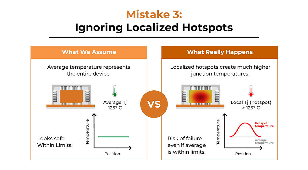
Thermal failures increasingly originate from small localized hotspot regions generated by localized interactions between electrical, magnetic and thermal phenomena. These hotspots frequently remain invisible during conventional thermal validation despite dominating long-term reliability behavior.
Modern switching architectures introduce several mechanisms that intensify localized heating:
Current crowding around vias and switching nodes
Skin-effect-induced copper losses at elevated frequencies
Proximity-effect heating inside compact busbar structures
Magnetic core saturation regions
Uneven current distribution across parallel semiconductor devices
Localized parasitic inductance concentration
As dv/dt and di/dt values increase, current distribution becomes increasingly nonuniform throughout PCB copper layers, package interconnects and bus structures. Current crowding elevates localized resistive losses while higher-frequency harmonics intensify conductor heating through skin and proximity effects.
Magnetics experience similar concentration effects. Compact high-frequency transformers and inductors often develop localized core-loss concentration due to nonuniform flux distribution and fringing-field interaction with nearby conductive structures.
The resulting thermal distribution becomes highly uneven.
Infrared thermal imaging may show acceptable average temperatures while small localized hotspot regions operate at substantially higher stress levels. These regions frequently become initiation points for long-term degradation mechanisms including dielectric breakdown, substrate fatigue and insulation failure.
This challenge becomes more severe under real operating conditions where airflow degradation, enclosure recirculation, altitude variation, vibration and contamination alter local thermal behavior dynamically.
High-voltage systems introduce additional electrothermal coupling effects. Elevated electric-field concentration combined with localized thermal stress accelerates dielectric aging and partial discharge initiation inside insulation structures. Once initiated, partial discharge progressively degrades dielectric integrity until catastrophic insulation failure occurs.
Thermal concentration and electric-field concentration are therefore becoming tightly coupled reliability mechanisms in compact high-voltage architectures.
Mistake 4: Separating Thermal Engineering from Switching Physics
One of the largest conceptual shifts occurring in modern power electronics is the realization that thermal behavior is increasingly governed by electromagnetic behavior.
Historically, electrical optimization and thermal optimization operated somewhat independently. Electrical engineers focused on switching efficiency, power density and transient response while thermal engineers concentrated on heat dissipation and cooling structures.
Wide-bandgap semiconductors are collapsing that separation.
Fast-switching SiC and GaN devices generate extremely high dv/dt and di/dt transients that directly influence localized thermal behavior through parasitic-driven energy concentration mechanisms. Switching-node compression, electromagnetic coupling and transient current redistribution alter heat-generation patterns throughout the package and PCB structure.
Higher switching frequencies improve efficiency and reduce passive component size, but they also compress heat generation into increasingly smaller spatial and temporal regions.
GaN devices illustrate this behavior particularly clearly.
Their lateral device structures and extremely low gate charge enable exceptional switching speeds and power density. However, the resulting transient behavior can create highly concentrated electric fields and localized energy dissipation regions that are difficult to model accurately using traditional thermal-analysis approaches.
Similarly, SiC devices tolerate elevated operating temperatures while simultaneously introducing stronger electric-field stress and faster transient dynamics across package insulation systems.
Parasitic inductance becomes especially important under these conditions. Even small parasitic inductance values can generate significant voltage overshoot and transient current redistribution during fast switching events. These transient interactions alter localized heating patterns across bond wires, copper structures and semiconductor junction regions.
Thermal behavior is therefore becoming inseparable from package parasitics, switching topology and electromagnetic field distribution.
This is driving increased adoption of coupled electrothermal simulation environments capable of evaluating transient switching behavior, parasitic interaction and thermal distribution simultaneously rather than independently.
Mistake 5: Designing for Nominal Efficiency Instead of Fault Survivability
Modern power-conversion systems are frequently optimized aggressively around nominal efficiency metrics. Under ideal operating conditions, these architectures often demonstrate exceptional performance.

Real operating environments behave very differently.
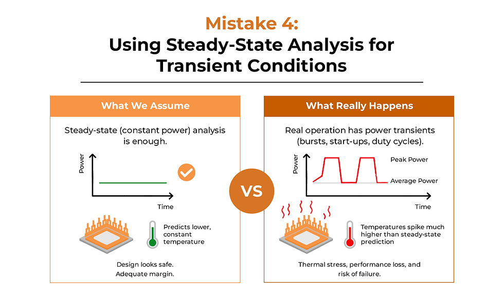
Transient overloads, regeneration events, unstable loads, short-duration fault conditions and rapid acceleration cycles introduce thermal stress profiles substantially different from nominal operation. During these conditions, thermal margins compress rapidly while localized electrothermal stress increases disproportionately.
This creates another major reliability misconception.
A converter achieving excellent steady-state efficiency may still possess limited thermal survivability under abnormal transient operation.
As power density increases, thermal tolerance margins shrink significantly. Design compromises that previously produced minimal impact now influence long-term reliability directly. Reduced copper thickness, compact package spacing, aggressive passive miniaturization and elevated switching frequencies all increase sensitivity to transient thermal accumulation.
Modern thermal engineering therefore revolves increasingly around controlled compromise rather than absolute optimization.
Higher switching frequency improves efficiency while intensifying thermal concentration.
Compact magnetics improve integration density while elevating hotspot generation.
Smaller enclosures improve packaging efficiency while reducing thermal spreading capability.
Faster transient response improves control performance while amplifying electrothermal stress accumulation.
The engineering objective is no longer maximizing a single parameter. It is balancing efficiency, thermal survivability, electromagnetic stability and lifecycle reliability simultaneously.
The thermal design assumptions governing previous generations of power electronics are being fundamentally reshaped by wide-bandgap switching behavior, elevated power density and compact converter architectures.
Modern failures increasingly emerge from localized electrothermal stress mechanisms developing gradually inside systems that appear thermally compliant under conventional validation methodologies. Heat density, transient thermal gradients, package parasitics and thermomechanical fatigue are increasingly joining average temperature as the dominant reliability constraints across EV infrastructure, aerospace electronics, industrial automation, renewable-energy systems and next-generation power-conversion platforms.
Thermal engineering is no longer a secondary mechanical discipline attached to electrical design. It is becoming one of the central architectural layers governing long-term system stability, field reliability and lifecycle predictability.
Advanced power electronics development extends well beyond individual component selection, with McKinsey Electronics supporting engineering teams through engineering-led design guidance and authorized access to high-reliability SiC and GaN semiconductor ecosystems. Support spans power semiconductors, gate drivers, passive components, thermal management, magnetics, interconnects and circuit protection technologies, enabling system-level optimization across switching performance, thermal dissipation, EMI mitigation, packaging constraints, lifecycle continuity, traceability and long-term supply assurance. This integrated approach helps organizations develop high-density, high-efficiency power systems that maintain reliable performance throughout development, production and long-term field deployment.