The Silent Revolution: How Ultra-Precise Wire Bonding is Reshaping Semiconductor Packaging
- May 22, 2025
- 5 min read
Updated: Aug 7, 2025
Read Below:
Strategic Role in Packaging Supply Chain: McKinsey Electronics supports the adoption of next-gen wire bonding by providing circuit advisory and chip equivalency services across the MENA region, Türkiye and Africa, thus bridging the gap between packaging innovation and real-world deployment.
Wire Bonding Reinvented: Once thought obsolete, wire bonding is experiencing a renaissance through ultra-fine pitch precision, alternative materials like copper and silver and emerging geometries such as ribbon bonding, making it a viable competitor to Flip-Chip and TSV.
AI-Driven Manufacturing: Advanced AI vision systems and self-learning bonding machines are transforming wire bonding into a high-yield, low-defect, cost-efficient interconnect solution for applications in automotive, RF, aerospace and beyond.
The Underdog That Refuses to Die
If you think wire bonding is dead, you’re missing one of the biggest revolutions in semiconductor packaging. For decades, industry experts have predicted that Flip-Chip and Through-Silicon Vias (TSV) would render wire bonding obsolete. As semiconductor devices pushed towards higher density and performance, the conventional wisdom was clear: wire bonding—once the workhorse of chip interconnects—was too slow, too bulky and too limited for the future.

Yet, something unexpected has happened. Rather than fading into obsolescence, wire bonding is experiencing a technological renaissance. Semiconductor giants are re-investing heavily in ultra-precise wire bonding techniques, leveraging its cost advantages, flexibility and newfound precision to compete with modern interconnect technologies.
With AI accelerators, 5G modules and automotive electronics demanding ever-more-efficient packaging solutions, the competition is fierce. Can wire bonding, a technology that has been around since the 50s, outmaneuver Flip-Chip and TSV for next-gen chip designs?

Let’s dive into the breakthroughs that are rewriting the rules of semiconductor packaging.
1. The Breakthroughs Bringing Wire Bonding Back
Sub-10μm Bonding Precision: The New Era of Fine-Pitch Bonding
One of the primary criticisms of wire bonding has been its pitch limitations. Historically, it lagged behind Flip-Chip in interconnect density. However, advancements in ultra-fine pitch bonding—with precision now reaching sub-10μm levels—are changing the game. New bonding machines can place wires with micron-level accuracy, allowing for significantly higher-density interconnects.
Material Science Evolution: Beyond Gold to Copper, Silver and Graphene
Gold has long been the standard for wire bonding due to its reliability and oxidation resistance. However, rising costs and electrical resistance concerns have driven a shift towards alternative materials:
Copper wire bonding is now mainstream, offering lower resistance, improved thermal performance and better electromigration properties.
Silver wire bonding is emerging as a high-performance alternative, delivering excellent conductivity at lower costs than gold.
Graphene and nano-enhanced wires are in early development, promising even higher thermal and electrical efficiency for future applications.
The Rise of Ribbon Bonding: Higher Current, Lower Resistance
Traditional round bonding wires are being replaced in some applications by ribbon bonding, which provides:
Lower electrical resistance due to its wider surface area.
Higher current-carrying capability—critical for power devices in electric vehicles and AI accelerators.
Improved thermal dissipation, reducing hotspot formation in high-power applications.
These material and geometric innovations mean that wire bonding is no longer just a legacy solution—it’s a cutting-edge technology competing with the most advanced interconnect methods.
2. The Great Interconnect War: Wire Bonding vs. Flip-Chip vs. TSV
The semiconductor packaging landscape is a battleground where three main interconnect technologies are competing for dominance. Here’s how they stack up against each other:
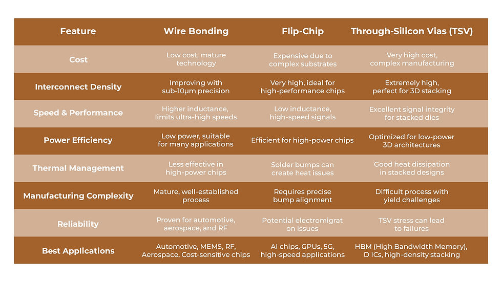
Where Wire Bonding Still Wins
Despite Flip-Chip and TSV advancements, wire bonding remains the preferred choice for:
Automotive electronics (long-term reliability)
MEMS and RF modules (cost-sensitive and performance-balanced)
Aerospace and military applications (proven durability)
With ultra-precise bonding techniques, wire bonding is proving to be a formidable contender in semiconductor packaging.
3. AI-Powered Bonding: How Machines Are Perfecting Precision
The resurgence of wire bonding isn’t just about materials and geometries—it’s also about AI-driven manufacturing.
Defect-Free Bonding with AI Vision Systems
Today’s wire bonding machines integrate real-time AI vision to detect misalignments and bonding defects at the sub-micron level. These systems use:
Machine learning algorithms to predict and correct bonding issues before they occur.
Automated process optimization that adapts wire placement dynamically.
High-speed defect analysis, reducing scrap rates and improving yield.
Self-Learning Bonding Machines: Precision at Sub-Micron Accuracy
AI-powered bonding machines now feature self-adjusting parameters, allowing them to:
Learn from past bonding cycles to improve accuracy
Adjust force, heat, and loop formation dynamically based on material properties
Optimize wire routing to minimize electromagnetic interference
Industry Impact: Lower Costs, Higher Yields
The integration of AI in wire bonding manufacturing means:
Higher yields, with near-zero defect rates.
Lower production costs, making wire bonding even more competitive.
Faster production cycles, improving throughput for high-volume manufacturing.

4. The Unexpected Future of Wire Bonding: Will It Dominate Again?
With continuous innovations in precision, materials, and AI integration, wire bonding is proving that it’s far from obsolete. But could it actually dominate semiconductor packaging once again?
Extreme Miniaturization: The Next Wire Bonding Challenge
As chips continue to shrink, wire bonding faces a challenge: maintaining reliability and conductivity in sub-5μm pitch applications. Researchers are exploring:
Nano-enhanced bonding materials to improve conductivity.
Hybrid bonding approaches that combine wire bonding with other interconnect technologies.
New encapsulation methods to enhance longevity and durability.

Integration with 3D Packaging: Hybrid Approaches
Rather than competing with 3D stacking, wire bonding is being integrated into hybrid packaging solutions. For example:
Fan-Out Wafer-Level Packaging (FOWLP) using wire bonding for cost-efficient interconnects.
Heterogeneous integration, where wire bonding links chiplets in advanced packaging designs.
Multi-die RF modules, combining TSVs, Flip-Chip, and wire bonding for 5G and aerospace.
These innovations could extend wire bonding’s dominance into new generations of semiconductor devices.
The Silent Revolution in Semiconductor Packaging
The semiconductor industry is obsessed with transistor scaling—but interconnect innovations are just as critical. While newer technologies like Flip-Chip and TSV have pushed packaging performance forward, wire bonding has quietly evolved into a precision powerhouse.
Ultra-fine pitch bonding is now rivaling Flip-Chip’s density.
New materials and geometries are improving conductivity and performance.
AI-driven bonding machines are making defect-free production a reality.
Far from being obsolete, wire bonding is adapting, evolving and proving its worth in next-generation chip designs.
While ultra-precise wire bonding is reshaping semiconductor packaging, its impact extends beyond manufacturers to distributors. As a key supplier in the MENA region, Turkey and Africa, we, at McKinsey Electronics play a critical role in ensuring that cutting-edge packaging technologies reach the right applications. With wire bonding maintaining a strong presence in automotive, RF and aerospace electronics, the demand for cost-efficient, high-reliability components remains high. McKinsey Electronics supports this transition by providing circuit design advisory services and chip equivalency solutions, helping engineers navigate the evolving landscape of interconnect technologies. As semiconductor packaging continues to advance, the right sourcing and expertise will be essential in integrating these innovations into real-world designs.


