From Fabless Innovation to Regional Deployment: Scaling Semiconductor Design in the KSA
- Apr 16
- 5 min read
Read Below:
Fabless semiconductor innovation in KSA is accelerating, but industrial impact depends on structured deployment, including validation, design-in engineering and supply chain alignment beyond tape-out.
Scaling across GCC, Africa and Türkiye requires system-level validation and regional adaptation, ensuring semiconductor performance under real operating conditions such as thermal stress, EMC and regulatory requirements.
Through its partnership with Rimal Semiconductor, McKinsey Electronics enables design-to-deployment execution, bridging local chip innovation with engineering integration and reliable multi-market scaling.

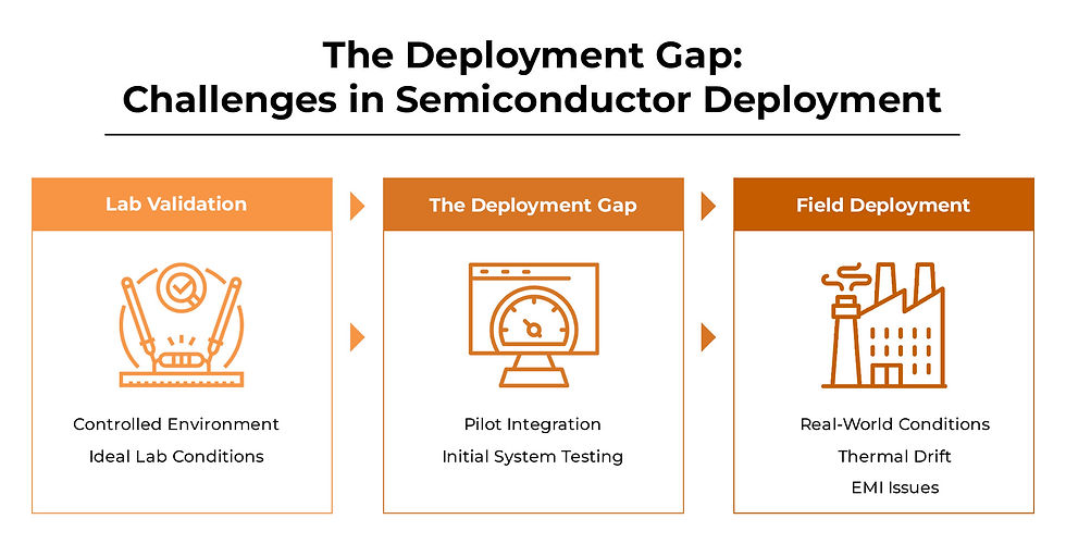
Semiconductor design capability is advancing rapidly across Saudi Arabia and the wider region. Under Saudi Vision 2030, fabless innovation is becoming a key component of industrial development. Yet design capability alone does not create industrial impact. Semiconductor innovation must be translated into validated, deployable systems that perform reliably under real operating conditions.
As fabless semiconductor companies expand across the Middle East and adjacent markets, the challenge shifts from innovation to execution. The question is no longer how to design silicon, but how to ensure that silicon integrates, scales and performs consistently across renewable energy systems, industrial platforms and electrified mobility architectures.

From Tape-Out to System Integration
The semiconductor lifecycle does not end at tape-out. Once a design is finalized and fabricated through global foundries, it enters a complex pathway toward deployment. This pathway includes testing, validation, integration and production alignment.
At the wafer level, parametric testing confirms that devices meet electrical specifications. Packaging introduces additional variables, including thermal resistance, parasitic inductance and mechanical integrity. These factors influence how the device behaves once integrated into a system.
System integration represents the first real test of design robustness. Semiconductor devices must interact with power architectures, control systems and environmental constraints. Switching behavior, thermal performance and electromagnetic compatibility become defining parameters at this stage.
Validation as a Deployment Gate
Validation is the critical bridge between design and deployment. It ensures that semiconductor devices perform as intended within real application environments.
In power electronics systems, validation extends beyond functional testing. It includes:
Thermal characterization under load conditions
Electromagnetic compatibility assessment
Power integrity and transient response analysis
Long-duration stress testing
Reliability and lifetime testing (HTOL, temperature cycling)
These processes confirm whether a design maintains stability across operating conditions typical of GCC environments, including high ambient temperatures and variable load profiles.
Validation also supports compliance with regional and international standards. Without structured validation, even technically sound designs face barriers to adoption.
Design-In Engineering and Early Engagement
Successful deployment begins before production. Design-in engagement ensures that semiconductor devices are aligned with system requirements at the earliest stages of development.
Engineering teams evaluate how a component interacts with the broader system. This includes PCB layout optimization, grounding strategies and filtering design to ensure stable operation. For high-frequency switching devices such as SiC and GaN components, layout inductance, gate drive design and switching loop optimization become key factors influencing performance.
Early engagement reduces the risk of redesign cycles. It allows system architects to account for thermal behavior, electromagnetic interactions and power distribution from the outset. This approach improves development efficiency and supports faster transition to production.
Supply Chain Alignment and Lifecycle Control
Scaling semiconductor deployment requires disciplined supply chain management. Availability, lifecycle status and sourcing stability directly affect production continuity.
Fabless companies rely on external foundries and packaging partners. This introduces dependencies that must be managed through forecasting, allocation strategies and supplier coordination. Component lifecycle monitoring ensures that products remain viable throughout their intended use. This includes proactive management of Product Change Notifications (PCN) and End-of-Life (EOL) transitions to prevent unexpected redesign or production disruption.
Engineering and supply chain functions must operate in coordination. Component selection decisions influence long-term availability and system stability. Structured sourcing strategies reduce the risk of disruption and support consistent production output.
Regional Deployment Across Diverse Markets
Expanding across GCC, North Africa, South Africa and Türkiye introduces additional complexity. Each region presents unique regulatory frameworks, environmental conditions and infrastructure maturity levels.
Semiconductor devices must perform across varying temperature ranges, electrical conditions and application requirements. Design validation must therefore consider a broader set of operating scenarios.
Regulatory compliance adds another layer. Certification requirements differ by market, and alignment must be achieved before deployment. This requires coordination between engineering, compliance and supply chain teams.
Regional deployment is not a linear process. It involves continuous adaptation and validation to ensure consistent system performance across diverse environments.
The Role of Authorized Distribution
Authorized distribution plays a central role in bridging semiconductor design with deployment. It provides the structure needed to connect innovation with application-driven commercialization.
Through its partnership with Rimal Semiconductor, McKinsey Electronics supports the transition from fabless design to regional deployment. This includes engineering engagement, validation support and supply chain coordination.
Field Application Engineers work closely with customers to align semiconductor functionality with system requirements. They validate performance under real operating conditions and support design optimization at the system level.
Distribution also ensures supply continuity. Forecasting, lifecycle monitoring and sourcing strategies maintain component availability across production cycles. This enables semiconductor solutions to scale reliably across multiple markets.
From Innovation to Industrial Impact
Semiconductor design capability represents the starting point of a broader industrial process. The ability to move from design to deployment defines the real impact of innovation.
In Saudi Arabia, this transition supports national objectives related to industrial diversification, technology development and regional leadership. By combining fabless design with structured deployment pathways, the Kingdom is building an ecosystem that connects innovation with execution.
The integration of design, validation, engineering support and supply chain management creates a foundation for scalable semiconductor adoption across high-growth sectors.

Scaling Semiconductor Design Across Emerging Markets
Emerging markets present both opportunity and complexity. Demand for advanced electronic systems is increasing across energy, mobility and industrial sectors. At the same time, deployment environments introduce unique challenges that require localized engineering approaches.
Scaling semiconductor design in this context requires a structured pathway:
Design aligned with application requirements
Validation under real operating conditions
Engineering-led system integration
Coordinated supply chain execution
This pathway transforms semiconductor innovation into deployable, reliable systems.
Supporting System Integration with Rimal Semiconductor Devices
Rimal Semiconductor solutions support deployment across energy, mobility and industrial systems through high-efficiency power devices including:
SiC MOSFETs for high-voltage switching
IGBTs for industrial motor drives
GaN devices for high-frequency power conversion
Power management ICs for system efficiency
These technologies enable reliable operation under demanding environmental conditions typical of GCC and emerging markets.
The expansion of fabless semiconductor design in Saudi Arabia marks a significant step in the region’s technological evolution. However, the value of design capability is realized only when it translates into production-ready systems.
Authorized distribution, engineering engagement and structured validation frameworks enable this transition. They ensure that semiconductor devices move from tape-out to deployment with consistency and reliability.
As Saudi Arabia strengthens its position within the semiconductor ecosystem, the ability to scale design across regional markets will define long-term success. The connection between innovation and execution becomes the foundation for industrial growth and technological leadership.